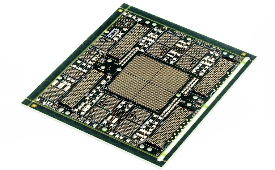
HDI PCBs are an integral part of modern electronic devices, especially those expected to provide high performance while consuming minimal power.
Compared to traditional PCBs, HDI PCBs, contain a high density of connections in a relatively small area for which a multilayer design is used.
To utilize the multilayer design, different types of microvias are used. HDI PCB manufacturing process is a complex process that requires careful consideration of multiple factors so that the end product meets all the performance criteria.
In this article, we will navigate the readers through the complete step-by-step process of the HDI PCB manufacturing process.
What is the HDI PCB Manufacturing Process?
The HDI PCB manufacturing process involves the use of laser drilling, sequential lamination, and advanced materials to create finer lines, micropores, and high-density connections.
HDI PCB can achieve a compact design with multiple layers, improving the signal integrity and performance of modern intelligent electronic products.
HDI PCB Manufacturing Process can be Divided into 4 Phases
The Design Phase
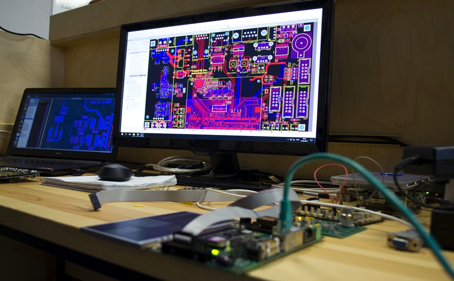
- Schematic Design: To take on HDI PCB manufacturing the very first thing to do is design it and for that, there are many great software’s like Altium, KICAD, and EasyEDA that provide all the necessary tools to prepare the final design. With the design software, the designers can specify the dimensions of the PCB, its layer count, the number and types of vias, trace width, and placement of the components.
- Material Selection: During the HDI PCB manufacturing process, selecting the right material for the PCB substrate depends on various factors such as operating frequency, dielectric constant, electrical chemical and thermal properties, glass transition effect, signal integrity, durability, cost, etc. The following table describes various PCB materials used in the HDI manufacturing process.
| Materials | Dielectric constant | Maximum Operating frequency | Thermal properties | Signal integrity | Cost |
|---|---|---|---|---|---|
| FR-4 | 4.2 - 4.8 | 3GHz | Tg ~ 130-180°C, moderate thermal conductivity | Moderate signal integrity, suitable for general applications | Low |
| Polyimide | 3.2 – 3.4 | 10GHz | Tg ~ 250-260°C, high thermal stability | High signal integrity, suitable for high-temperature environments | Moderate to High |
| Metal Core PCB (MCPCB) | 4.5-7.0 | 2GHz | Excellent thermal conductivity, good heat management | Moderate signal integrity, ideal for high-power applications | Moderate |
| Rogers 4350B | 3.66 | 20GHz | Tg ~ 280°C, high thermal stability | High signal integrity, ideal for RF/microwave applications | High |
| PTFE (Teflon) | 2.1 | 50GHz | Tg ~ 200-260°C, excellent thermal stability | Superior signal integrity, used in high-speed and RF designs | Very High |
- Layer Stackup: An HDI PCB is made up of multiple layers these layers usually come in the stack configuration of 4, 6, and 8 but for the sake of simplicity these layers can be divided into ground layer, power layer, and signal layer. During the design process, all these layers should be designed to be adjacent to each otherwise the layers will wrap up during HDI PCB fabrication.
Fabrication Phase

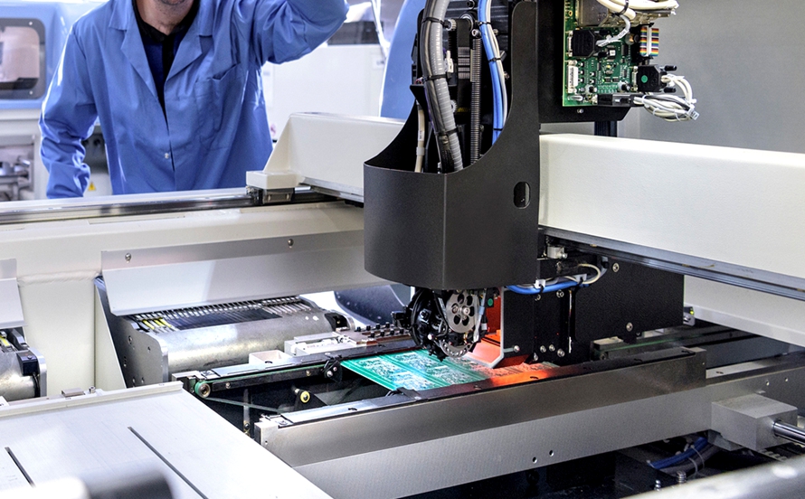
The HDI PCB fabrication is much more complex than the traditional PCBs because HDI PCBs are made up of multiple layers and each layer goes through various fabrication processes and then all the layers are joined together in the lamination phase. the processes that each layer goes through are pretty much similar and are as follows:
- Photoresist Application: On the PCB substrate (which is coated with a thin sheet of copper) a film of light-sensitive material called a photoresist is applied in the HDI PCB manufacturing process, and then an image of the circuit is projected on the substrate. Due to the effect of light photoresists get hard over the circuit image and the rest of the soft photoresist is removed.
- Etching: After the application of photoresist, the substrate is dipped into an etching solution which dissolves all the copper over the substrate except the copper covered with hardened photoresist. After the etching, a copper circuit is formed on the substrate and then the photoresist is removed and the substrate is cleaned with a neutral solution to remove any traces of the etchant.
- Computer-Aided Optical Inspection: After etching a picture of the circuit on the substrate is taken and compared with the picture of the original design to check for any errors in the HDI PCB manufacturing process with the help of computers. If no error is found in the HDI PCB fabrication, the substrate is passed to the next process.
- Copper Lamination: The copper layer present on the substrate from the beginning is very thin and thus cannot withstand the higher current applications to make the copper layer thicker the substrate is dipped into copper sulfate solution and to speed up the process current is passed through the copper layer and copper from the copper sulfate starts depositing on the circuit and the copper layer gets thicker controlling the amount of current and time in the solution helps in getting the desirable thickness.
Lamination Phase
Lamination is an important PCB manufacturing process in which all the layers of PCB are stacked on top of each other and bonded together but before that, holes are drilled on these layers, and layers with buried vias are laminated first for this purpose. To start the lamination all the PCB layers are cleaned and stacked on top of each other and a prepreg is put between them then heat and pressure is applied which melts the prepreg and all the layers get joined to form one piece of PCB. Once all the layers are combined and since buried vias are already made other vias such as blind, through-hole vias are drilled with high-precision drilling tools. After that, the board is covered with a resin to protect the copper traces from oxidation and then the PCB goes through HASL (Hot Air Solder Levelling) where the PCB is dipped into a molten solder bath due to which a layer of solder is formed on the pads.
Quality Control and Testing Phase

After HDI PCB fabrication and lamination, the PCB goes through rigorous tests to ensure it is working properly and to identify defective ones coming from the assembly line. Those teats are as follows:
- Visual Inspection: The complete PCB is inspected by a technician for any damage on the board such as scratches and misalignment of layers after HDI PCB electronics manufacturing.
- Electrical Testing: In electrical testing probes are placed on every point to check continuity and shorts this method of probing is good for small-scale HDI PCB manufacturing but at large the bed of nails technique is used where a fixture that has nails is placed on the board and those nails act as probes to check the board for continuity and shorts
- X-Ray Testing: X-ray testing is another important step in HDI PCB electronics manufacturing. In this technique, X-rays are used to check the solder joints. This technique is especially useful for checking buried vias and proper solder joints that are hidden under the top layers.
- Environmental Testing: Environmental testing is essential in the HDI manufacturing process. Here the PCB is made subject to various environmental factors such as high heat, moisture, mechanical stress, etc to determine its performance under extreme circumstances.

